Poster Session I
EDP1-1
Single photon event camera for fast target tracking
13:30-15:00 Dec.3
*Sai-Ying Ru1, Qing-Yuan Zhao1,2
Research Institute of Superconductor Electronics (RISE), School of Electronic Science and Engineering, Nanjing University, Xianlin Avenue, Nanjing, Jiangsu, 210023, China1
Purple Mountain Laboratories, Mozhou East Load, Nanjing, Jiangsu, 211111, China2
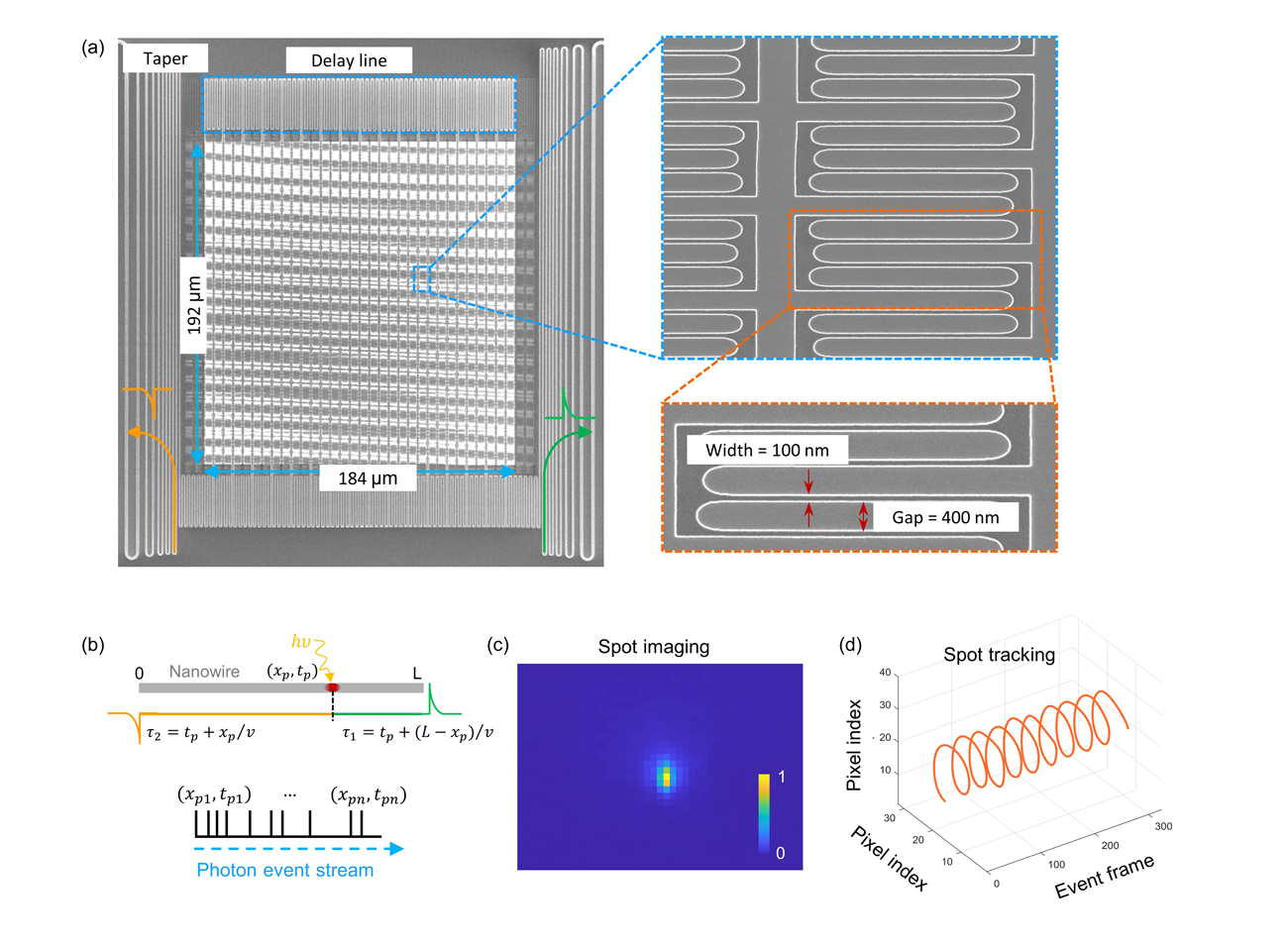
Dynamic target tracking involves continuously monitoring and following a moving object or entity over time to determine its position, velocity, and trajectory. This process is crucial in many applications where understanding and predicting the movement of targets is essential. Since position of the object is unknown, a camera equipped with a detector array is used. Conventional detector arrays, such as CCDs or CMOS arrays, operate based on the sequence of readout logic. Thus, the imaging speed, i.e. frame rate, is determined by the clock of readout lines. In single-photon detection regime where the detection event is sparse and random, readout efficiency of conventional frame-based camera is low since most pixels have no photon counting. Therefore, an event camera that can be triggered by each photon detection is required to maximize the imaging speed. Here, we introduce a kilopixel single-photon delay-line imager, which naturally operates in event-driven mode. The imager was fabricated using superconducting nanowires, which was designed in parallel structure and then meandered into a two-dimensional array over an area of 184 μm × 192 μm. It had 32 columns and the equivalent rows were 40 determined by the differential time jitter. Based on this imager, a single-photon event camera for fast target tracking was built. The imager was placed in a 1 K free-space coupling cryostat. An aspheric lens was placed on a cryogenic XYZ-nano-positioner at 4 K to focus the light onto the imager. The maximum system efficiency was 56.2% at 1550 nm and the time jitter was 200 ps. At room temperature, a galvanometer was used to provide feedback control of the tracking process. With this camera, single-photon trajectory tracking at a high speed of 1 kHz was achieved.
[1] Zhao, Q.-Y. et al. Single-photon imager based on a superconducting nanowire delay line. Nat. Photonics 11, 247–251 (2017).
Figure 1. (a) SEM images of kilopixel single-photon delay-line imager. (b) Conceptual illustration of photon event readout by the imager. The photon arrival time tp and position xp can be obtained by the arrival time of a pair of positive and negative pulses. (c) The imaging of the focused light spot. (d) Single-photon trajectory tracking demonstration.
Keywords: Kilopixel single-photon delay-line imager, Photon-triggered event camera, Fast dynamic target tracking
EDP1-2
Superconducting kinetic inductance detectors with photon noise limited sensitivity at terahertz waveband
13:30-15:00 Dec.3
Tianyuan Chi1, Lili Shi1, Runfeng Su1, Siming Zang1, Rui Tan1, Shiyi Yao1, Yuwei Zhu1, JunhuaChen1, Jingbo Wu1,2, Xuecou Tu1,2, Biaobing Jin1,2, *Jian Chen1,2, Peiheng Wu1,2
Research Institute of Superconductor Electronics, School of Electronic Science and Engineering, Nanjing University, Nanjing 210023, China1
Purple Mountain Laboratories, Nanjing 211111, China2
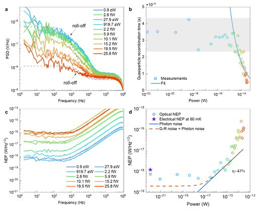
The terahertz (THz) waveband is of immense interest in astronomy as it encompasses significant energy generated following the Big Bang, offering critical insights into processes invisible in other bands, such as the earliest stages of planet, star, and galaxy formation. Superconducting kinetic inductance detectors (KIDs) have emerged as a formidable contender in the field of THz astronomy, attributed to their exceptional sensitivity and scalability [1,2]. In this study, we introduce a novel class of KIDs incorporating a lumped element (LE) superconducting resonator design, with inductors fabricated on β-Ta film and capacitors on α-Ta film. We characterize the noise of the hybrid α-Ta/β-Ta LEKIDs, achieving an optical noise equivalent power (NEP) of 4.8 × 10⁻¹⁹ W/Hz1/2, demonstrating high sensitivity (Fig.1). Additionally, the LEKIDs exhibited robust stability across multiple thermal cycles. The combination of high sensitivity and robust stability makes the hybrid LEKIDs promising for the stringent demands of astronomy and other applications at THz waveband.
[1] Ulbricht G., De Lucia M. & Baldwin E., Applications for Microwave Kinetic Induction Detectors in Advanced Instrumentation, Appl. Sci., 11, 2671 (2021).
[2] Su R. F., et al. Noise equivalent power of a NbTiN-Al-based kinetic inductance detector for terahertz sensing, Supercond. Sci. Technol., 35, 055016 (2022).
This work was supported by the National Key Research and Development Program of China (2021YFB2800701), the National Natural Science Foundation of China (Nos. 62227820, 62035014, 62071217, 62331015).
Figure 1. Measured noise PSD and optical NEP of the hybrid α-Ta/β-Ta LEKID. (a) Measured noise PSD at different radiation powers. The measurements were performed at 60 mK, and the readout power is -100 dBm. The Lorentz fit (dashed line) is used to get the quasiparticle recombination time. The roll-off frequency at higher (lower) and lower (higher) radiation power are shown as the arrows, respectively. (b) Quasiparticle recombination time extracted from the Lorentz fit of (a). The circles denote the measurement data. The blue solid line is a power law fit (Popt-0.5), ignoring the data in the saturated regions (the first 14 points). (c) Measured optical NEP of the LEKID at different radiation power. The lowest NEP is 4.8 × 10⁻¹⁹ W/Hz1/2. (d) Measured optical NEP at different radiation powers and the calculated photon shot noise with a 43% optical efficiency. The NEP is average between 30 and 50 Hz from (c). The blue star is the measured electrical NEP at 60 mK, which corresponds to a radiation power of 3.4×10⁻²² W. The solid green line indicates the calculated photon shot noise with a 43% optical efficiency. The red dashed line is the sum of photon shot noise and G-R noise. The measured NEP is well fitted with the noise limits between 3×10-17 W and 3× 10-15 W. After that, the LEKID is gradually saturated, leading to a deviation to the photon shot noise limit.
Keywords: Superconducting detector, Kinetic inductance detector, Photon noise limited sensitivity, Terahertz waveband, Noise equivalent power
EDP1-3
Improved operating current margin of the Josephson voltage standard by supplying the bias current with a long Josephson junction
13:30-15:00 Dec.3
*Hirotake Yamamori, Daiki Matsumaru, Michitaka Maruyama, Chiharu Urano and Nobu-Hisa Kaneko
National Institute of Advanced Industrial Science and Technology, 1-1-1 Umezono, Tsukuba, Ibaraki 305-8563 Japan
The quantum voltage standard realizes D/A conversion by many Josephson junctions in series, and the junction array is implemented by folding it many times on the chip. The superconducting current concentrates on the inner circumference of the wiring, and the apparent critical current of the Josephson junction decreases due to the influence of the asymmetrical current bias. At first glance, this decrease in current is difficult to distinguish from that due to magnetic flux trapping. Unfortunately, this reduces the width of the Shapiro step and reduces the operating current margin of the D/A conversion. This problem becomes even more severe for superconducting materials with higher critical temperature such as NbN, which have a large magnetic penetration depth.
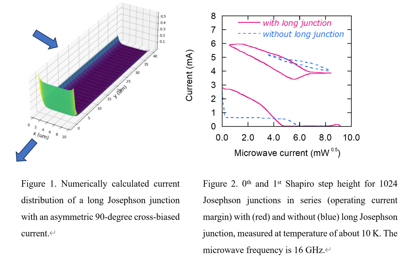
To prevent this current concentration, several ways have been proposed, such as thickening the film thickness in the current concentration area [1] or making the inner circumference jagged so that its physical length is equal to the outer circumference [2]. We propose a more effective method that is easier to implement. By placing a junction with a critical current larger than the bias current in the current concentration area, this junction is affected by the current concentration in the wiring, but since the critical current is sufficiently larger than the current flowing in the circuit, it functions as a superconducting wiring. Figure 1 shows the numerically calculated current distribution of a long Josephson junction with asymmetric 90-degree cross bias current, which shows that the current is concentrated on the short side, providing a symmetric current to the Josephson junction array. Figure 2 experimentally shows that the operating current margin is significantly improved, which suggests the junction array with the long Josephson junction is effective in preventing the effect of current concentration due to bending of the wiring.
[1] J.M. Xiong at al., SuST, 35, p.055015 (2022).
[2] H. Kim at al., IEEE TMTT, 57, pp.442-448 (2009).
This research was supported by the New Energy and Industrial Technology Development Organization (NEDO) under project “JPNP19005.”
Keywords: Josephson Voltage standard, Josephson junction array
EDP1-4
A high efficiency superconducting nanowire single-photon detector at 10 μm wavelength integrated with a membrane optical cavity
13:30-15:00 Dec.3
*Jie Deng1, Qing-Yuan Zhao1,2
Research Institute of Superconductor Electronics (RISE), School of Electronic Science and Engineering, Nanjing University, Nanjing, Jiangsu, 210023, China1
Purple Mountain Laboratories, Nanjing, Jiangsu, 211111, China2
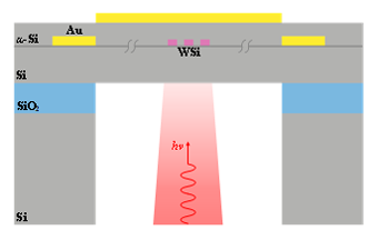
Recently, superconducting nanowire single-photon detectors (SNSPDs) have been demonstrated to achieve saturate quantum efficiency at longer wavelengths up to 20 μm [1]. However, the detection efficiency of the reported devices was relatively low due to the small detection area and a lack of an efficient optical cavity. Here, we demonstrate a high-efficiency SNSPD integrated with a membrane optical cavity to increase the light absorption at 10 μm. The nanowire was made from 5 nm thick WSix film with a critical temperature of 2.68 K, showing a well saturated quantum efficiency at 10 μm. To increase the output signal amplitude, both avalanche detector structure and an impedance-matched readout were used. The nanowire was fabricated on a SOI wafer. After a backside etching process, only the top 2 μm thick silicon layer was remained. Combined with an addition silicon layer and a top gold mirror deposited on top of the nanowire, a membrane Fabry-Perot (FP) cavity was built. Simulation results indicated that this cavity can reach a maximum light absorption of 26.08 % at 10 μm. The detection efficiency was measured in a free-space coupling 300 mK cryostat, which was 20.69% at 10.18 μm. With this device and a tunable QCL pulsed laser, response spectrum from 8 μm to 12.5 μm and polarization dependence was measured. In addition, a 2×2 detector array using delay-line readout was also demonstrated.
[1] Gregor G., Alexander B.et al. Low-noise single-photon counting superconducting nanowire detectors at infrared wavelengths up to 29 µm, Optica 10, 1672-1678 (2023).
Figure 1. A diagram of the membrane cavity designed for 10 μm superconducting nanowire single-photon detector.
Keywords: Superconducting nanowire single-photon device (SNSPD), Mid-infrared, Fabry-Perot (FP) cavity, Free-space test system
EDP1-5
Monolithic integrated superconducting nanowire digital encoder and its application in reading out a SNSPD array
13:30-15:00 Dec.3
*Yanghui Huang1, Qingyuan Zhao1,2
Research Institute of Superconductor Electronics (RISE), School of Electronic Science and Engineering, Nanjing University, Nanjing, Jiangsu 210023, China1
Purple Mountain Laboratories, Nanjing, Jiangsu 211111, China2
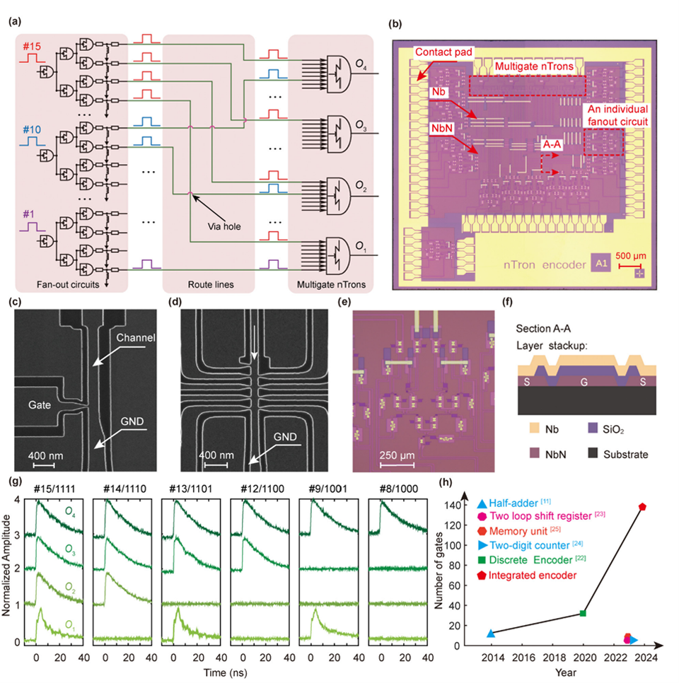
As reported in the IEEE International Roadmap for Devices and Systems 2022 (IRDS), superconducting digital circuits are one of the most promising technological method due to their exceptional operational speed and low power consumption. Superconducting nanowire cryotron (nTron) is a three-terminal device with a feature size of around 100 nanometers, fabricated by superconducting thin films. When a current is injected into the gate, the channel is transited from superconducting state to highly resistive normal state, which enables nTron to generate an amplified output pulse governed by gate input.
Attribute to its high output impedance, transistor-like operation logic and low power consumption, nTrons have been demonstrated in driving low-temperature COMS transistors, building neural networks, reading out low-temperature detector arrays, etc. Exploring nTrons in digital integrated circuits and quantum circuits is promising but faces challenging in scalability. In this study, we demonstrate a monolithic integrated nTron-based binary encoder, which includes input fanout circuits, on-chip biasing, combinational logic routing and multi-gate nTrons. This monolithic nTron digital circuit comprises 137 nTron gates, 424 resistors, 274 inductors, and 64 vias, which is developed using a two-superconducting-layer fabrication process. The maximum bias margin is 28% for the fanout circuit and 60% for the multi-gate nTron when using a signal generator, while the minimum timing jitter is 40 ps. The total power dissipation mainly from biasing resistors is 19.6 μW, making it more power efficient than RSFQ encoders. This nTron encoder is used to digitize and read out a 15-pixel SNSPD array, of which the fired pixel position is encoded into 4-bit address, which shows a minimum readout error rate lower than 10-4 and reduces the readout RF lines from 15 to 4.
[1] Huang, Y.-H., Zhao, Q.-Y., Chen, S., Hao, H., Wang, H., Guo, J.-W., Tu, X.-C., Zhang, L.-B., Jia, X.-Q., Chen, J., Kang, L., & Wu, P.-H. (2023). Splitter trees of superconducting nanowire cryotrons for large fan-out. Applied Physics Letters, 122(9), 092601.
[2] Huang, Y.-H., Zhao, Q.-Y., Chen, S., Hao, H., Wang, H., Guo, J.-W., Tu, X.-C., Zhang, L.-B., Jia, X.-Q., Chen, J., Kang, L., & Wu, P.-H. (2023). Splitter trees of superconducting nanowire cryotrons for large fan-out. Applied Physics Letters, 122(9), 092601.
The authors have no conflicts to disclose.
Figure 1. Overview of the 4-bit encoder. (a) Schematic diagram of the encoder. (b) Microscope image of the monolithic nTron encoder. Scanning electron microscope images of a single-gate nTron (c) and a multi-gate nTron (d). (e) Microscope image of the fanout circuit. (f) Conceptual diagram of the multilayers for cross section A-A0 marked in (b). (g) Output waveforms for input ports #15/1111, #14/1110, #13/1101, #12/1100, #9/1001, and #8/1000. The waveforms are normalized and vertically shifted on the y axis for clarity. The waveform of O1 has a second rising edge overlapped on the first one, which is unusual in the case of the other three outputs. It is possibly caused by a fabrication defect along the channel of that multi-gate nTron, where the hotspot growth becomes discontinuous. (h) Trend of the number of gates in nTron digital circuits over reported time.
Keywords: Superconducting nanocrytron, Integrated encoder, Bit error rate, Superconducting nanowire single-photon detector (SNSPD) array.
EDP1-6
Locating nanoscale inhomogeneities in a superconducting nanowire by probing and mapping self-heating hotspots
13:30-15:00 Dec.3
*Zhen Liu1, Qing-Yuan Zhao1,2
Research Institute of Superconductor Electronics (RISE), School of Electronic Science and Engineering, Nanjing University, Xianlin Avenue, Nanjing, Jiangsu, 210023, China1
Purple Mountain Laboratories, Mozhou East Load, Nanjing, Jiangsu, 211111, China2
In the field of high-sensitivity single-photon detectors, superconducting nanowire single-photon detectors (SNSPDs) are widely used due to their excellent performance. The quasi-2D structure of superconducting nanowires introduces inherent nanoscale inhomogeneities that significantly impact device performance. For example, the dark count phenomenon in SNSPDs is believed to be closely related to these inhomogeneities. Traditional characterization methods, such as AFM and SEM, can visualize geometric shapes, surface morphology, composition, or superconducting energy gaps, but have not yet revealed the direct relationship between these inhomogeneities and electrical transport performance.
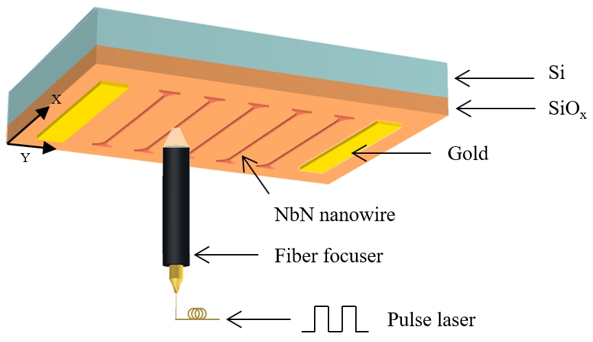
This study proposes a method for investigating random inhomogeneities in superconducting nanowires by probing and mapping self-heating hotspots. We mounted a fiber focuser on a 3-axis cryogenic nano-scanner to focus and scan a laser spot on a superconducting NbN nanowire. Localized hotspot can be generated within a maximum distance of ~300 nm triggered by the laser. The associated self-heating IV curve that revealed the shrink of the hotspot was collected and then be used for extracting information of inhomogeneities, such as geometry variation and spatial distribution. Furthermore, this method allowed us to locate where dark counts were generated along the nanowire. The number of dark count locations increased as temperature rose. A total number of eight dark count locations were observed at a temperature of 4 K. This method not only reveals the intrinsic inhomogeneities hidden in a superconducting nanowire, but also serves as a useful tool for investigating nanowire’s electrical and optical performance associated with inhomogeneities.
[1] Dane, A., Allmaras, J., Zhu, D. et al. Self-heating hotspots in superconducting nanowires cooled by phonon black-body radiation. Nat Commun 13, 5429 (2022).
[2] Skocpol, W. J., Beasley, M. R. & Tinkham, M. Self-heating hotspots in superconducting thin-film microbridges*. J. Appl. Phys. 45,4054–4066 (1974).
[3] Andreev, V. et al. Dark Counts in SNSPD Studied With Spatial Resolution. IEEE Trans. Appl. Supercond. PP, 1–5 (2024).
Figure 1. A diagram of focusing and scanning a laser spot on a superconducting NbN nanowire. The optical fiber was mounted on a 3-axis cryogenic nano-scanner to achieve precise scanning.
Keywords: Superconducting nanowire, Self-heating hotspots, Self-heating current, Nanoscale inhomogeneities, Dark counts
EDP1-7
Fabrication of self-aligned superconducting nanostrip photon detector with He ion irradiation
13:30-15:00 Dec.3
*Shin Kawaguchi
Kitami Institute of Technology
Recently, post processing using helium ion irradiation has attracted attentions to improve the performance of superconducting nanostrip photon detector (SNSPD) [1]. The post processing requires to use of SNSPDs with front-illuminated structure rather than back-illuminated structure. Here, we report the fabrication of SNSPD with frontside illuminated and self-aligned structure. NbTiN and MoN were used as superconducting materials. MoN is known to be a good candidate for high-performance SNSPDs [2]. Ultrathin films of NbTiN and MoN with a thickness of 10 nm were grown using the magnetron sputtering, and the films were processed into meandering fine wires with a linewidth of 100-200 nm using conventional electron beam lithography and reactive ion etching. Then they were cut into disk shapes with a diameter of 2.5 mm using deep etching with SF6 and C4F8. After the fabrication, the device characteristics were optimized using He ion irradiation, and the focusing position was self-aligned by inserting it into an optical fiber sleeve with an inner diameter of 2.5 mm. SNSPDs with saturated detection efficiency were obtained.
EDP1-8
Evaluation of transmission efficiency of HTS bulk resonator antenna with director for wireless power transfer
13:30-15:00 Dec.3
*Hiroki Akimoto1, Yuki Ikezu1, Yuki Ikezu1, Ikuto Shindou1, Masafumi Shibata2, Shunya Suzuki1, Yuzuru Narita1, Takao Oto1 , Atsushi Saito1
Graduate School of Science and Engineering, Yamagata University, Japan1
Fuji Electric Co., LTD., Japan2
Recent research on microwave wireless power transmission has shown that the transmission efficiency of 60% can be achieved by using normal-conducting patch antenna arrays (88) at 28 cm with 1 dB of conductor loss at the antenna [1]. To reduce the conductor loss, it is effective to use a superconductor for the antenna materials. We recently proposed, designed, and fabricated an antenna using HTS bulk to improve the power handing capability of conventional superconducting antennas [2], but the transmission efficiency of the HTS bulk resonator was lower than the level reached in previous studies [1]. To improve the transmission efficiency, the antenna directivity must be improved, which might be possible by arraying or loading directors [3]. There are currently no reports of HTS bulk resonator antennas with directors.
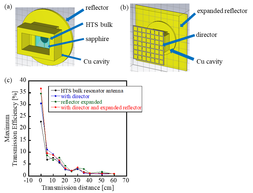
In this paper, we evaluated the transmission efficiency of the HTS bulk resonator antenna with a director for wireless power transfer. For this propose, first, we designed the HTS bulk resonator antenna with a director using CST Microwave Studio. Fig. 1(a) shows the model of the HTS bulk resonator antenna, and (b) shows the model of the HTS bulk resonator antenna with the director and the expanded reflector area. Second, we fabricated the director on the basis of the simulated results. Finally, we measured the HTS bulk resonator with and without the director and reflector and evaluated the transmission efficiency. For preparing the HTS bulk antenna, the HTS bulk and fabricated PTFE to implant the HTS bulk and feed port were parceled by substrates made using c-sapphire plate. After that, the substrates and SMA connector were placed in the bottom of the Cu cavity, and the upper part of the Cu cavity was set to the bottom one. The director was fabricated by cutting FR-4 substrates into square shapes. The director was loaded by spacers made of the PTFE. The bottom of the Cu cavity was used by the reflector, and when expanding the reflector area, the square Cu plate was placed in the bottom of the Cu cavity. We carried out the measurements in an anechoic chamber. The antenna was cooled to about 48 K by using a pulse tube cryocooler.
Fig. 1(c) shows the dependence of the transmission efficiencies on the transmission distance measured using a vector network analyzer and a commercially available horn antenna as a receiver antenna. With the HTS bulk resonator antenna used as a transmission antenna, the transmission efficiency was 22.8% when the transmission distance was 0 cm, and with the HTS bulk resonator using the director and expanded reflector, it was 36.8%. These results indicate that the HTS bulk resonator with the director and expanded reflector is effective for improving the transmission efficiency.
[1] T. Tomura et al., IEEE Open Journal of Antennas and Propagation, Vol. 2, pp. 170-180, 2021.
[2] K. Ehara et al., Electronics and Communications in Japan, Vol. 82, pp. 55-69, 1999.
[3] S. Arao et al., Proceedings of the conference on Electronics mounting, Vol. 20, pp. 139-141, 2006.
Some of this work was performed in the clean room at Yamagata University.
Figure 1. (a) Simulation model of HTS bulk resonator antenna. (b) Simulation model of HTS bulk resonator antenna with the director and expanded reflector. (c) Comparison of transmission efficiency with and without director and reflector.
Keywords: Antenna, HTS, Wireless Power Transfer
EDP1-10
Error Reduction Method of an RSFQ Approximate Multiplier Using Double Operations
13:30-15:00 Dec.3
*Shogo Kato, Nobutaka Kito
Chukyo University, Toyota, Aichi, 470-0393 Japan
Rapid single-flux-quantum (RSFQ) circuits are gaining attention as ultra-fast and low-power computing devices. Multiplication is a fundamental arithmetic operation extensively used in scientific and technical applications, including artificial intelligence processing. Multipliers consume a large layout area. Minimizing the area of a multiplier to embed many ones in a chip is essential to improve computational performance. Therefore, many compact RSFQ multipliers have been investigated. Recently, approximate computing emerged as a technique to reduce circuit area. Several RSFQ designs utilizing approximate computation have been proposed. However, they introduce errors in computational results. A mitigation method is essential for critical parts in numerical error.
This presentation proposes a method to reduce error by double operations of the approximated multiplier presented in [1]. This multiplier calculates an n-bit integer multiplication in 2n cycles and outputs the upper n-bits of the integer multiplication result. It is suitable for multiplications with a smaller bit width. The method improves the accuracy of n-bit approximate multiplication results to 2n-bits using the approximate multiplier twice.
The method calculates the product of two integers, X and Y, in three steps. First, an approximate multiplication of X and Y is carried out with the approximate multiplier [1]. Then, an approximate multiplication of X's reversed bit order and Y's reversed bit order is carried out. Finally, the result is obtained by subtracting the reversed bit order of the latter result from the former.
This presentation also discusses circuit implementations of the proposed method. The method's multiplication can be realized using one or two approximate multipliers. The clock cycle latency of the latter case is almost the same as the original multiplier's latency, and the former's latency is almost double of the original multiplier's latency. This presentation discusses RSFQ circuit realizations for the subtraction in the final step for both cases.
The absolute error of results obtained with the proposed method was evaluated with exhaustive patterns through simulation for 4- to 6-bit multiplications. The evaluation results show that 70% of multiplication results are the same as the accurate multiplication results in 4-bit.
[1] N. Kito, R. Odaka, and K. Takagi, “Rapid Single-Flux-Quantum Truncated Multiplier Based on Bit-Level Processing,” IEICE Trans. Electronics, vol. E102-C, no. 7, pp. 607-611, 2019.
This research was supported by JSPS KAKENHI Grant Number JP22K11961.
Figure 1. Steps of the error reduction method using double approximate (approx.) multiplications.
Keywords: RSFQ circuits, Multiplier, Approximate computing
EDP1-11
2.4 Gbps laser communication based on a high-speed superconducting nanowire single photon detector array
13:30-15:00 Dec.3
*Fan Yang1, Qing-yuan Zhao1,2, Jian Chen1,2
Research Institute of Superconductor Electronics (RISE), School of Electronic Science and Engineering, Nanjing University, Xianlin Avenue, Nanjing, Jiangsu, 210023, China1
Purple Mountain Laboratories, Mozhou East Load, Nanjing, Jiangsu, 211111, China2
Superconducting nanowire single-photon detectors (SNSPD) provide high efficiency and high speed, especially in optical communication system operating in low-flux conditions, such as deep-space. Further increasing the counting rate for achieving higher communication rate requires multi-pixel SNSPD arrays to overcome the kinetic inductance reset time limit of a conventional SNSPD. However, the number of readout lines would increase the complexity in signal processing and synchronization.
Here, we demonstrate a four-quadrant (2×2) array, covering an detection area of 10μm × 10 μm. Each quadrant detector was designed into a 3-pixel serial architecture. Each pixel was on-chip shunted with a 30 Ω resistor. This array was installed in a low-vibration 1.5 K cryostat and coupled through a single-mode fiber lens placed on a cryogenic 3-axes nanopositioner. All four quadrant detectors showed saturated quantum efficiency. By aligned the focused light on one quadrant detector, the maximum system detection efficiency reached 94%. The width of detection pulses was ~5 ns. At higher counting rate, pulses started piling up, which can be reconstructed after post processing. With this high efficiency and high speed detector array, laser communication experiments were demonstrated at a data rate of 2.4 Gbps in the format of pulse position modulation.
[1] Hao, H., Zhao, QY., Huang, YH. et al. A compact multi-pixel superconducting nanowire single-photon detector array supporting gigabit space-to-ground communications. Light Sci Appl 13, 25 (2024).
Figure 1. Detector architecture and performance. a. Stucture of the high-speed SNSPD. b. System detection efficiency versus bias current for the first quadrant detector.
Keywords: Superconducting nanowire single-photon detector, System detection efficiency, Single photon communication
